In which I decide to take on a crazy project.
I’m graduating this weekend! For the second time! That isn’t the point of this post though, that will be for a different post that is probably happening next week. Graduating is relevant to this post though, it means that I will have a lot of free time for the next few weeks before my job starts, roughly 2 and a half months to be exact. I wanted a project to fill this space, and I wanted it to be bigger than an project I’ve attempted before.
So, plunging into the deep end, I have decided to make the P18240 out of 74XX logic chips!
Why in the world would you want to do this? What is the P18240? What are 74XX logic chips? How are you going to make an attempt at this that is even somewhat sane? All reasonable questions, so lets get to them in order:
But Why?
I’ve been at Carnegie Mellon for 5 years now, and for 3.5 years (seven semesters!), I’ve been involved with TA’ing the class 18-240: Structure and Design of Digital Systems. To say I enjoy this class would be an understatement, I took took 18-240 (240 as its shortened to in my department) during the second semester of my freshman year, and it opened my eyes to the concepts of digital design, FPGAs and hardware description languages. I was instantly enamored with how the course built our knowledge of digital design up from nothing. We covered basic gates, then we used those gates to make components, then we learned how to design larger ideas using those components at register transfer level logic, then we finally ended the course by working through designing a microprocessor (The P18240) together in lecture.
The thing that really made me love the course though was how nothing was a mysterious black box of “just trust us” (besides some aspects of FPGA synthesis, but thats reasonable). Everything that was taught to us was built upon things we had already seen before, including the processor we built at the end. At the time this was a huge leap for me because the only architecture I had worked with had been x86, which isn’t really friendly to understanding it’s construction. Over the years as I TA’d the course I got much more familiar with every aspect of the curriculum, including the P18240 and its design. While I haven’t had the opportunity to survey a wide variety of computer architectures, I’ve learned enough to know that the P18240 is weird, but when paired with the rest of the course, provides an easy no-nonsense way to build up to a whole microprocessor from components.
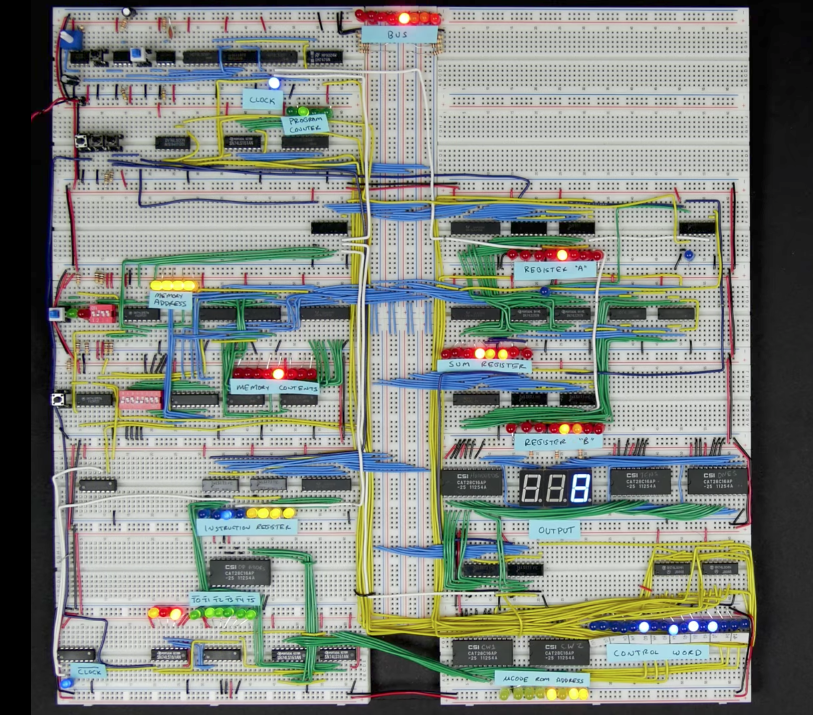
Anyway, as I looked for a summer project, I stumbled onto this video series on Reddit about how to build a 8 bit computer out of logic chips. It really caught my eye, and I had a lot of thoughts: “Could it really be that small?”, “Its really cool how you get to see the state in those LEDs!”, but most importantly, “I can probably build that!”.

|
But what fun would it be to simply follow some youtube tutorials and end up with something that is distinctly not my own? I put the thought of making the 8 bit CPU aside and went on looking for other ideas, but while grading 240 homeworks one night it hit me. I could make the P18240 in the same way that guy made the 8 bit computer! After all those years of TA’ing, I felt some odd connection to this quirky micro-architecture, though I had only ever interacted with it through Verilog and on an FPGA, forms that seemed easy to work with, but not something I could take with me when I left CMU. I wanted to make some representation of it that would last forever (or at least a long time). I wanted to make something that could be put in a corner in the lab and students could see their programs that they’ve written run on real hardware. And so, all of a sudden it was decided, my summer project would be bringing the P18240 into the real world.
The P18240

|
** Its important to take most of what I say in this section about computer architecture with a grain of salt. I never took a comp-arch course in my time at college, and so I only know what I’ve learned through the internet and other people. **
I was talking with my friend the other day about micro-architectures and he ended up making this comparison between RISC-V and MIPS, and how if MIPS is like english with its complexity and exceptions to certain rules, then RISC-V is like spanish: A nice set of rules, a good set of possible things to do with those rules, and relatively few, but consistent exceptions. While I cannot speak to the veracity of that claim, I wish to extend the simile a bit further and I would go so far as to say that the P18240 is like esperanto: Engineered to have no irregularities, but because it is too different, and not useful enough for any particular application except teaching, nobody besides our course uses it. Now, its important to take this comparison with a grain of salt. I never took a comp-arch course in my time at college, and so I only know what I’ve learned through the internet and other people, but I couldn’t resist putting the comparison in.
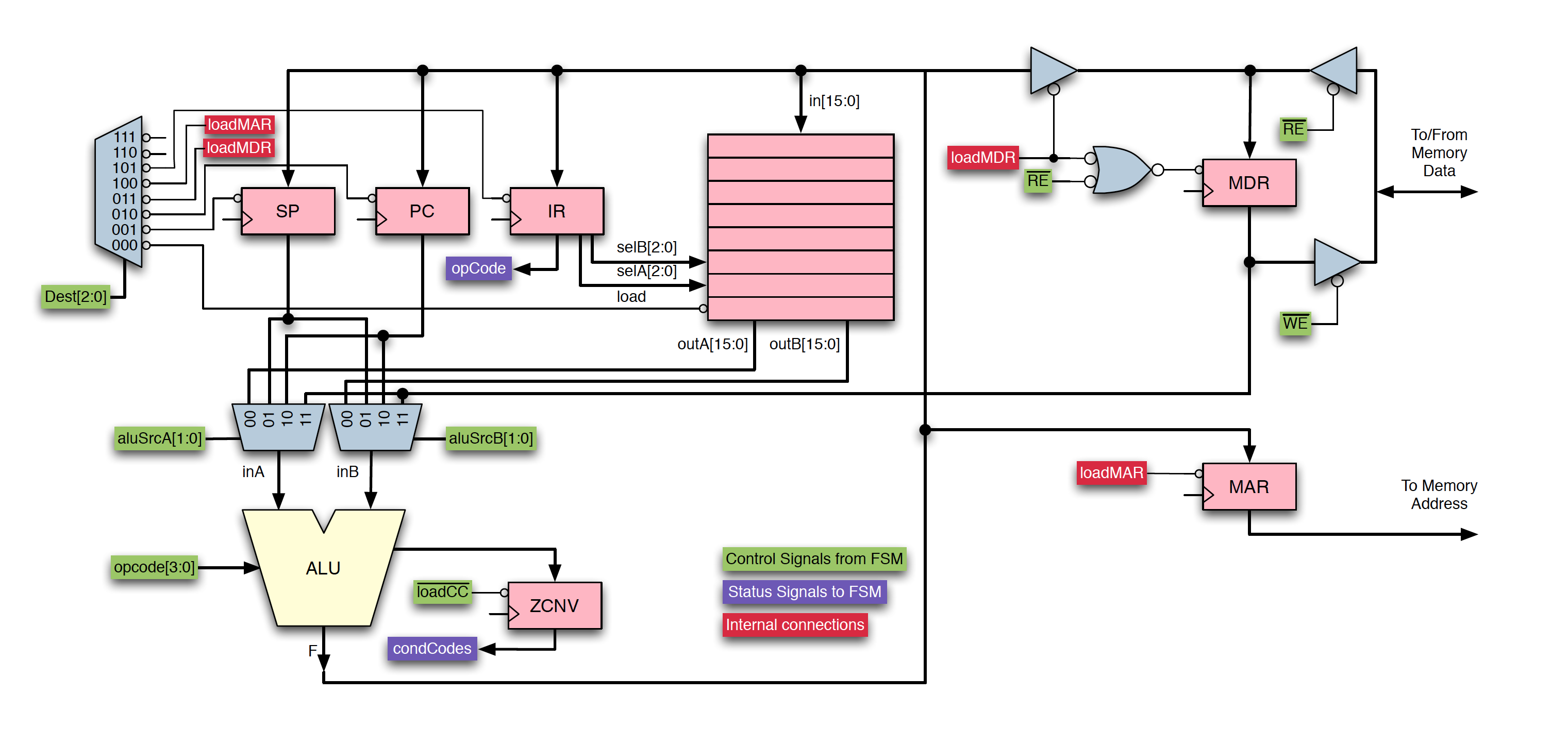
To start the description, the P18240 is a 16 bit architecture with 8 general purpose registers, a program counter (PC), stack pointer (SP), instruction register (IR) and an Arithmetic Logic Unit (ALU) with 16 possible operations. Each instruction is made up of 4-10 “micro-instructions”, each of which take one clock cycle to complete. The whole operation is guided by a finite state machine (FSM) that steps through the micro-instructions for each macro-instruction, providing various control signals to various parts of the architecture. Memory is accessed via a Memory Access Register (MAR) and a Memory Data Register (MDR), with reads and writes both assumed to take only one clock cycle. The general flow of data is that data can come from one of four sources (SP, PC, registers, or memory), the data will go through the ALU possibly performing some operation or possibly a no-op, and then being loaded into one of SP, PC, IR, MDR, MAR, or a register. You can find the full documentation on the project page and I’ll likely talk about each part in more detail as I implement it, so I’ll hold on all the gory details for now.
74XX Logic
So I have this weird architecture that I’m really dedicated to, what exactly am I claiming I’m gonna do with it?
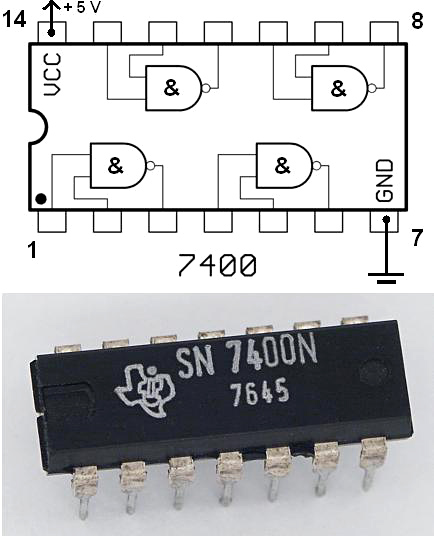
Way back when, Texas Instruments put out a series of chips called the 7400 Series logic chips (sometimes called 74XX chips). These copied the previously released 4000 series functionality of implementing most basic gates with some other special purpose chips while improving on the 4000 series by using TTL logic instead of CMOS logic. While the use of these chips has widely fell out of use today, some people will still include them in random places when a specific piece of functionality like a Multiplexer or Bus Driver is needed. They have also gained a popularity among people attempting to make old hardware as they implement most basic gates in varying sizes (thats me).

|
The series of chips is surprisingly flexible, with almost every gate in 2-input, 3-input, and 4-input varieties, a number of common components like D-flip-flops, multiplexers, adders, comparators, and some very large single purpose blocks of logic like seven segment display controllers. These are the tools that I have at my disposal for this project, and with the exceptions I’m about to get into, I think they will be more than enough.
But How?
So I’ve explained a bit about the P18240, and also a bit about the building blocks I’m using, and from that standpoint it could look like this is just a colossal undertaking. You would be right, but probably not to the extent you were thinking.
The goal that I am holding myself to is “To make the P18240 entirely out of 74XX chips, with the exception of the power supply, the clock, memory, various passive components, and anywhere that would be ‘completely unreasonable’ to use just 74XX chips.” Despite this being my project and me being allowed to do whatever I want with it, I really want to keep it ‘pure’. I could just simulate this whole thing with a microcontroller, but that would not just defeat the point but smash it to bits.
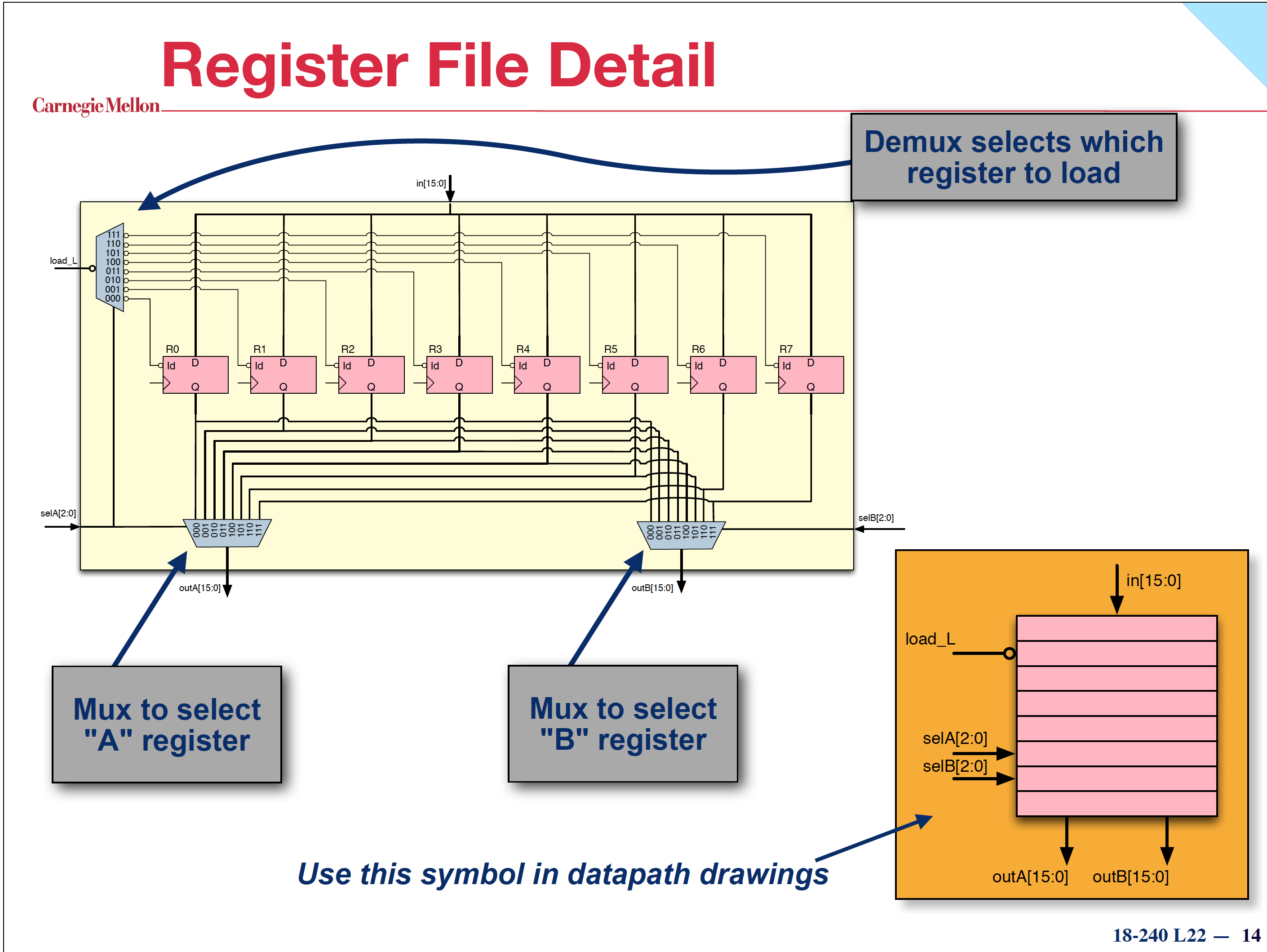
A brief glance over the P18240 reveals a few places that might warrant cheating the spirit of the goal, namely the ALU, the control FSM, and maybe the memory interface. I won’t truly know until I implement them whether or not these will need to bend the rules, but each would certainly provide a large challenge if attempted using solely basic gates and components. In addition, I plan on fudging the design in a few places as well. For example, a design based purely on the lecture slides would have me put multiplexers in the register file to select which registers are being output to the ALU.

|
Unfortunately, that would be an 8 input multiplexer with each input being 16 bits. The logic on that would be huge even using the 7400 series multiplexer chips because they only go up to two 4-bit inputs in size. So what I’m doing to avoid this problem here and in a few other places is turning the register output into a bus with drivers driven by a decoder controlled with what would be the select line to the multiplexer. It achieves the same effect, but is smaller overall and breaks the design up into a smaller part on each register rather than another large circuit blob.
So breaking up what I need to make into parts, I get:
- A register
- The ALU (including flags)
- The register file controller
- The memory interface
- Memory
- The controlpath FSM
- Overall control logic (enables and such)
- Connection circuitry for buses
I also need a few external controlling pieces of logic:
- Clock generator
- Output circuitry
- Program flasher
- Maybe memory mapped IO?
While subject to change, my current mental design has a circuit board for each of the above components, with 16 pin connectors and cables to connect them all. I hope to have it be able to lay out in a final rough rectangle for framing and display. Ideally it would also have LEDs to show component status in as many locations as possible. Basically I want this to be something that will be easy to assemble, easy to fix, look good, and be easy to display.
So…. Thats it…… I hope to make at least one post about each of those above parts, and will probably end up making a few posts about the parts I struggle with.
Lets see how this goes…
- Dillon