In which I revise my design to death.
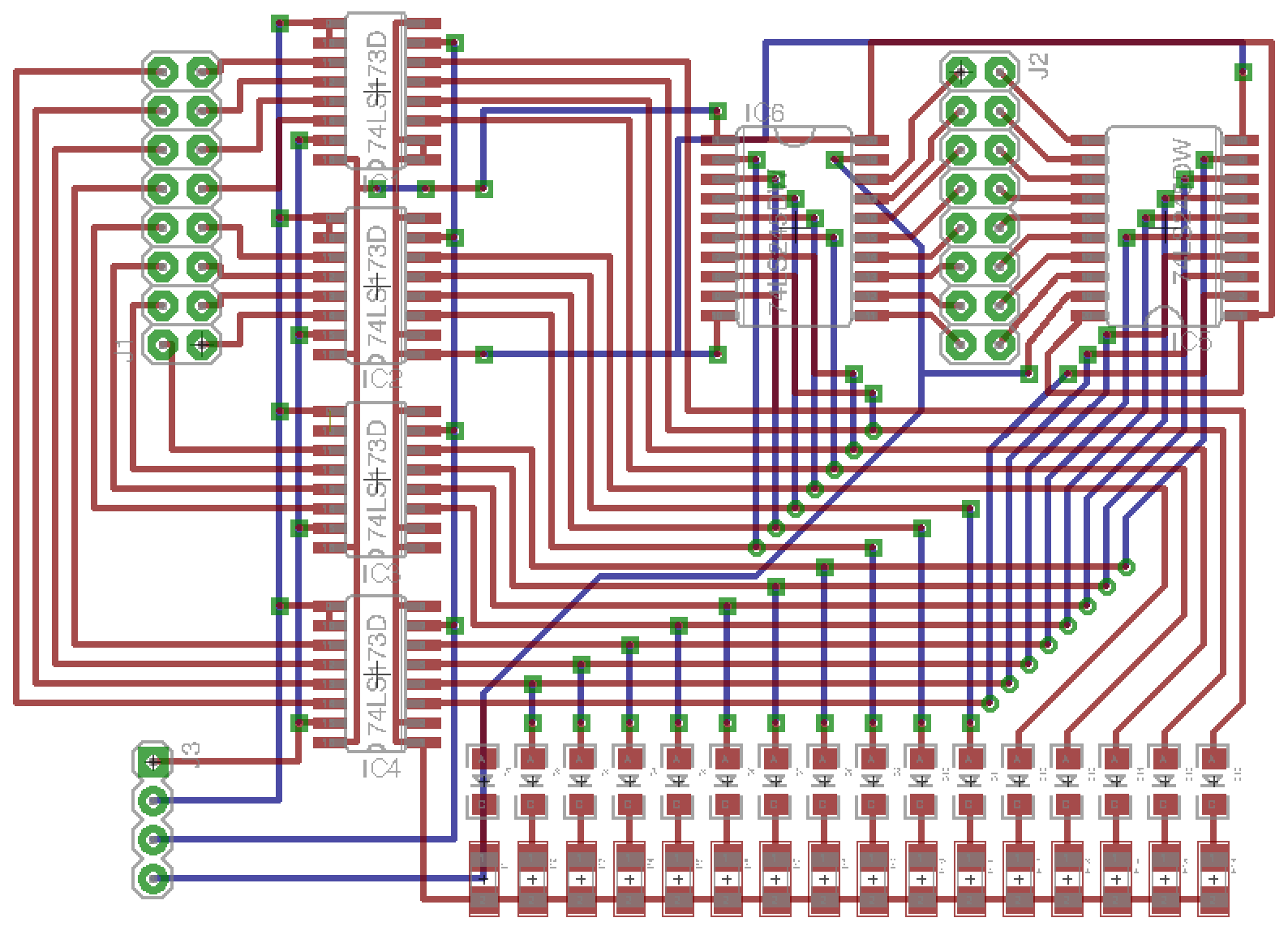
Left off the last post with a halfway decent schematic and no layout for the basic register. I unfortunately didn’t take any documenting pictures when doing the board layout, but here is what I ended up with:
|
I was pretty happy with this for a first layout. I had gotten the flow that I wanted, which is to say signals coming in from the left and leaving to the right, as well as 16 LEDs indicating the status horizontally. I had also designed it around having both the input and output connector at the same height, but I’m not sure what that really afforded me.
I immediately had some regrets as well, it seemed bulky and filled with mostly traces. Additionally I didn’t like the way I had to use up so much space because I chose a 2x8 connector and now everything had to get to both sides of the connector.
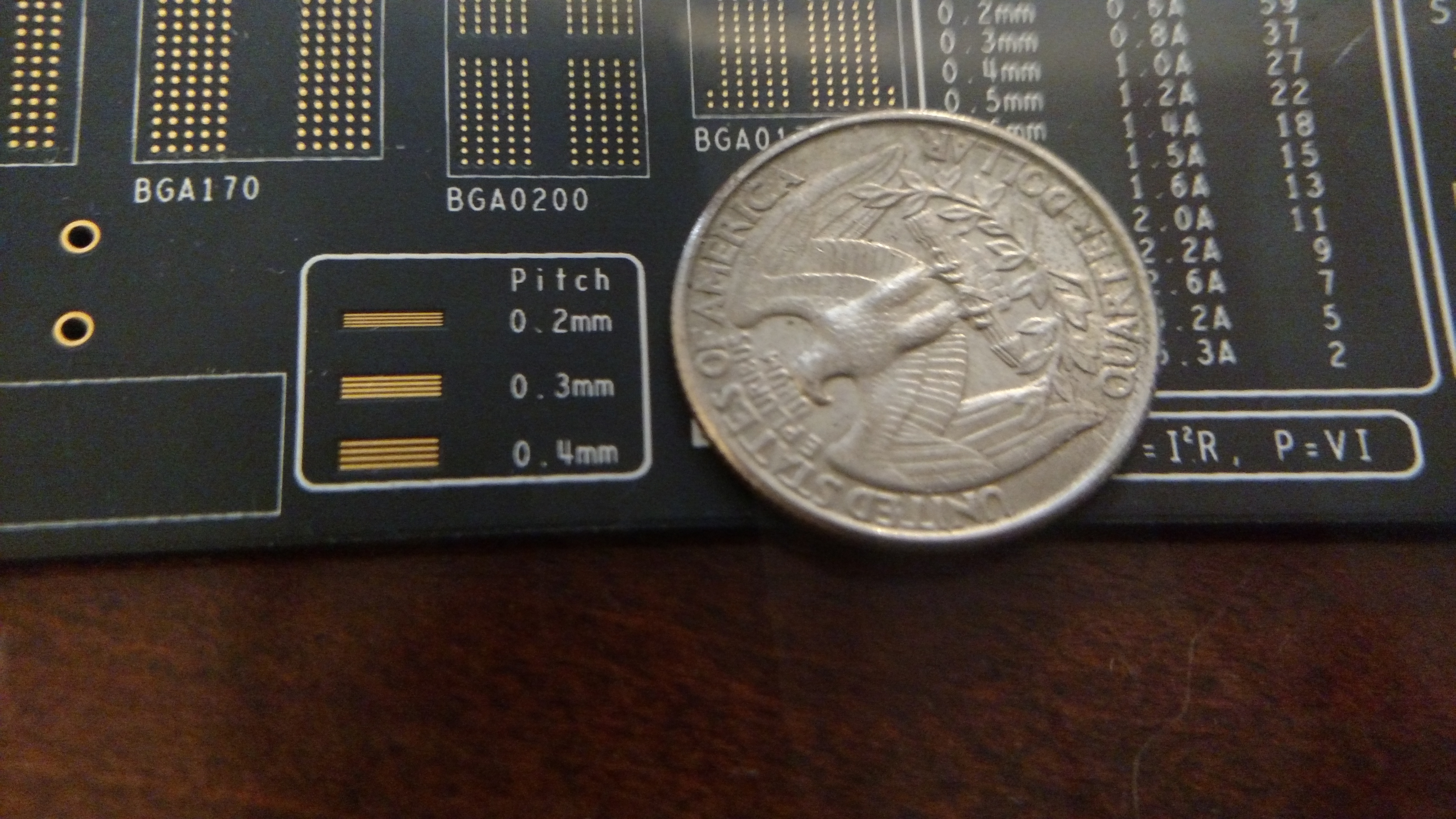
As for the issue of the board being mostly filled with traces, I figured it was a mixture of me being too cautious about trace spacing and laying things out poorly. I went to a few possible board houses and found that most reputable places have a minimum spacing of 6 mil (0.1524 mm). I had thought I had been using what were very small traces at 16 mil, but it turns out the industrial world continues to amaze me. After looking at my PCB sample ruler, I thought to myself that there was no way 6 mil traces could carry the current I wanted in all cases, and in addition I didn’t exactly trust all of the board houses I looked at to meet their minimum spec perfectly. So I took a trip to an online trace width calculator and after adding a rather large factor of safety I settled on a very reasonable 10 mil traces for most things and 20 mil traces for power in my revised design.
|
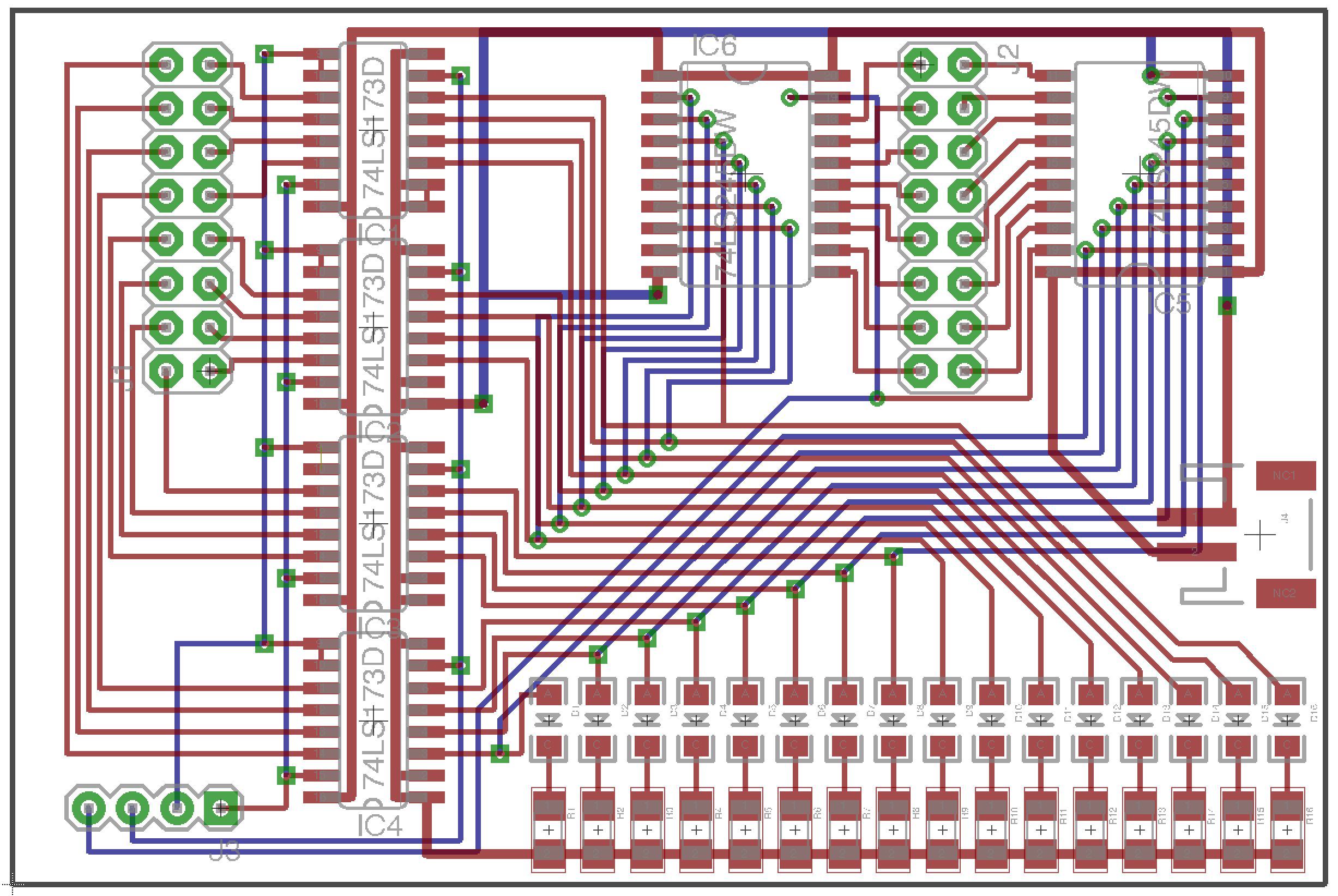
So overall for the revised board I shrunk the trace size, changed up the layout ever so slightly because of the smaller traces, and added a power connector that I had neglected to put in previously (whoops). Here is what that ended up looking like:
|
Overall the board size went down from 3.3” x 2.4” to 3” x 2”. It still didn’t sit perfectly with me, “I could go smaller!” I thought to myself. After thinking for a while about what could be done, I decided it was either the connector or the LEDs holding me back. Not wanting to compromise on the LEDs by getting rid of them, reshaping their layout, or making them harder to solder (they were already going to be a pain) I turned to the connector. I briefly thought about making the connector a 1x16 pin header but decided that would be unwieldy and also too large. So I did what any person in search of an answer would do, I typed “various electronics connectors” into google and browsed for roughly half an hour at all the different connectors I could get. I ended up liking FFC (Flat Flexible Cable) connectors the best, finding them the appropriate mix of small, probably not gonna break, and well known enough to purchase easily.
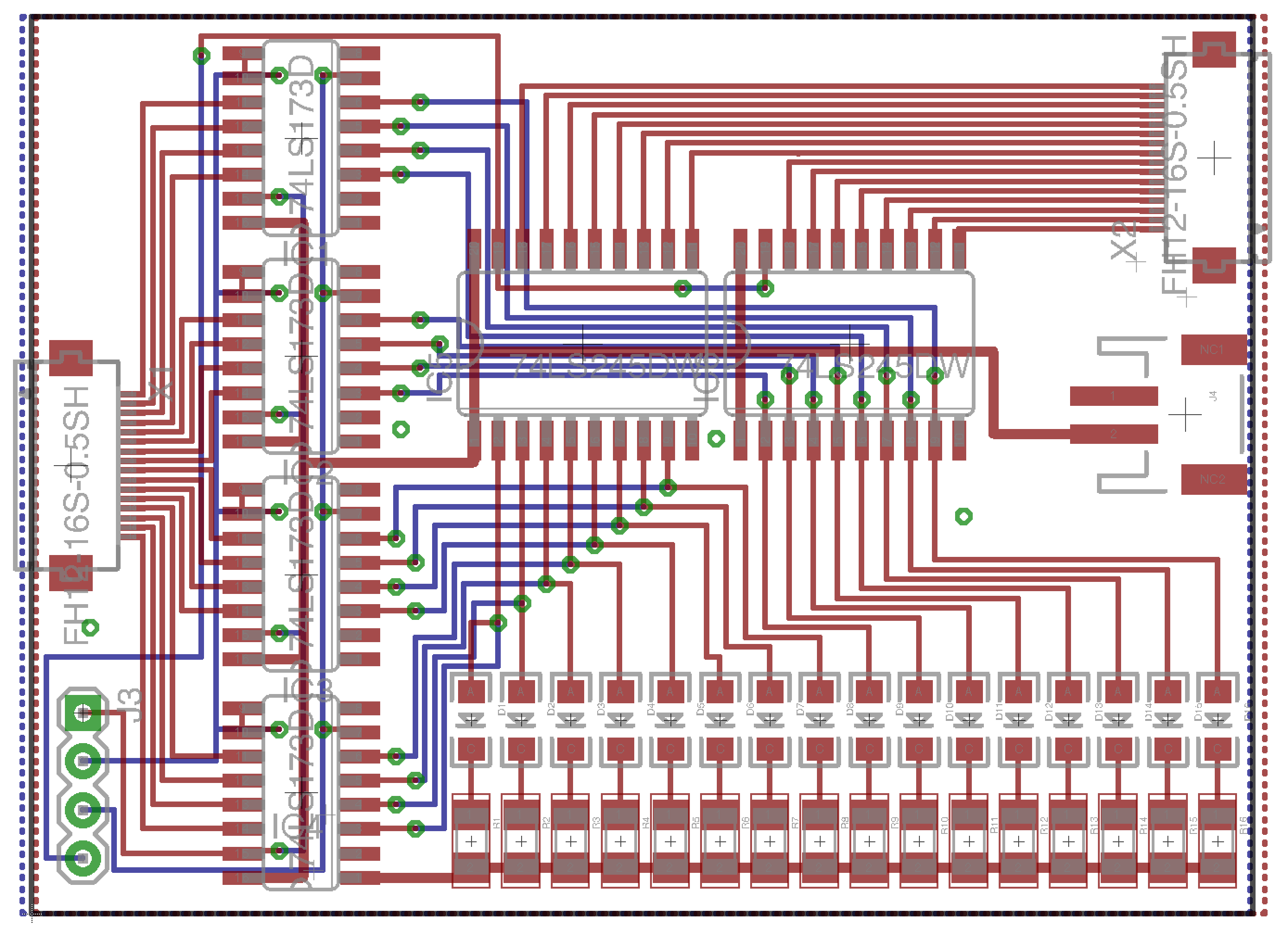
So I made a third version. In this version I basically did a complete re-layout, and I think it really helped.
|
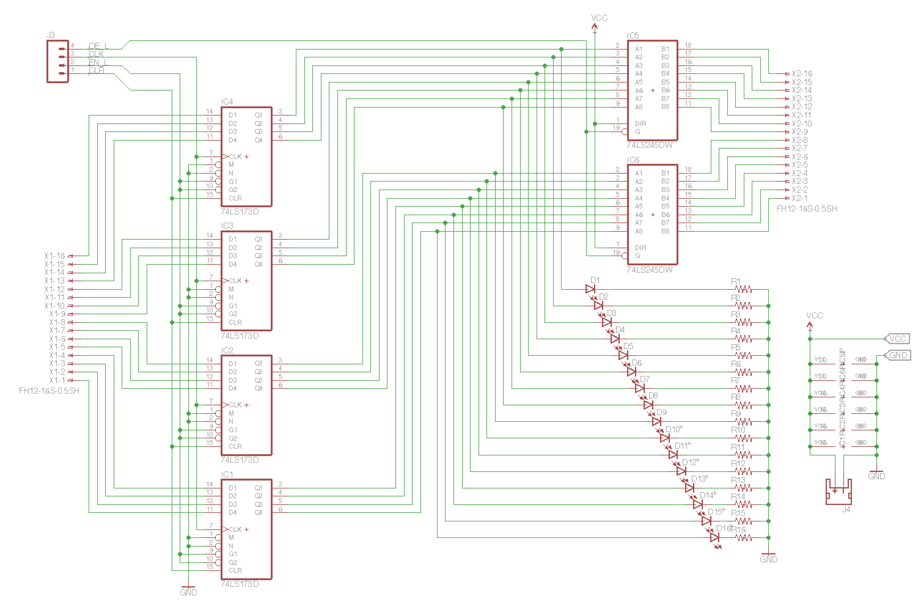
Whether or not the board shrunk much (from 3” x 2” to 2.6” x 1.86”) I really like the idea of these new connectors and the fact that I don’t need to get to both sides of the connector, it really made layout easier. It also made the schematic layout nicer.
|
The only bad thing is that because they are definitely directional, I can’t just flip them without putting pin 16 on the opposite side. This unfortunately means that somewhere in the design, pin 16 needs to flip from being on the bottom to on the top of the PCB. This is done on this board with the somewhat subtle diagonal crossover to the bus driver chips, but I wonder how it will translate in future designs. Ignore this, I realized I was completely wrong about this, check out the next blog post where I fix it.
The other thing that really helped this layout that I had blanked on the first time was having ground planes. I forgot how nice it is not having to worry about running ground traces.
I still have a bunch of thoughts about this design though:
- Need to add helpful silkscreen labels
- Despite the ideas of left to right flow, it would probably be smaller easier, and fit more nicely with the rest of the design to have both connectors on the left side of the PCB. I could then put the LEDs vertically on the right saving space, or rotate the row of 4 bit registers sideways.
- Is a random 4 pin connector still the best way to do control signals? What will that look like in the final design.
- Did I make the LEDs to small or too close together? Could I go smaller/closer?
For now though, this is enough that I will move on to a different and bigger part of the chip, the ALU! Keep an eye out for a blog post about an SMD test kit, it should hopefully let me gauge how small I can go with these SMD parts.
- Dillon