This should have been the first step.
A quick note: I know I’ve been writing a lot about this project, but short of some work on the ALU, the blog is now caught up to the work I’ve actually done, so expect some posts about other (possibly more interesting) things in the coming weeks. Back to the project though:
When I conceived this project, I mentally split the project into parts:
- Registers
- The ALU (including flags)
- The register file controller
- The memory interface
- Memory
- The controlpath FSM
- Overall control logic (enables and such)
- Connection circuitry for buses
- Clock generator
- Output circuitry
- Program flasher
I figured that each of these parts could individually designed to meet the same specification they meet in the class description and then joined without hassle (or at least with little hassle). That assumption might have even been correct if I hadn’t made some inherent modifications to the design…
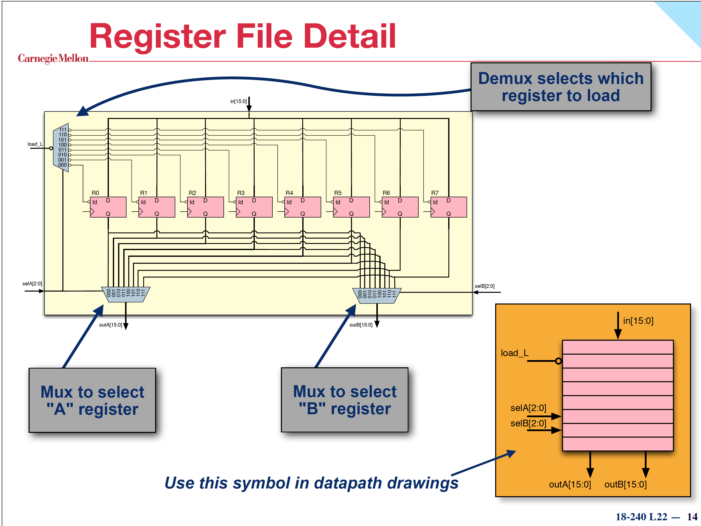
In addition, I plan on fudging the design in a few places as well. For example, a design based purely on the lecture slides would have me put multiplexers in the register file to select which registers are being output to the ALU.
Unfortunately, that would be an 8 input multiplexer with each input being 16 bits. The logic on that would be huge even using the 7400 series multiplexer chips because they only go up to two 4-bit inputs in size. So what I’m doing to avoid this problem here and in a few other places is turning the register output into a bus with drivers driven by a decoder controlled with what would be the select line to the multiplexer. It achieves the same effect, but is smaller overall and breaks the design up into a smaller part on each register rather than another large circuit blob.
- Me, in my first P18240 blog post.

|
The problem with making this modification is that the register file has two concurrent outputs. As such, in order to join all of the registers together as needed in the original specification, each register must be capable of independently writing to two buses. This means two sets of bus drivers on the register board itself. If you’ve been reading these blog posts in order, you’ll note that I spent quite a while revising the design of the register, now only to find that I’ll have to redesign it again. The upside is that this dual output register will also do well for the stack pointer and program counter registers which have to output to both inputs of the ALU independently because I’ve replaced a mux there as well.
Despite the re-designing that will have to happen and the difference from the design it causes, I still claim that the bus idea is a good idea. Each of the two multiplexers for the register file would have taken 28 (16+8+4) chips to implement, and each of the ALU muxes would have needed 12 (8+4 chips), meaning a total of 80 chips (282 + 122) to implement the system with muxes. Meanwhile, for the bus solution, each register only needs 4 chips, leading to a total of only 52 chips to implement the system with bus drivers.
Well, now that I’ve cleared up how I messed up the register design, lets not do it again by getting the rest of this system planned out. I struggled a lot with these design decisions. If the point of the system was strictly functionality, re-usability, or any metric based goal, the decisions might be easier, however my goals are (in this order):
- It accurately replicates the functionality of the P18240
- It is easy to recognize the separate parts of the design and see their status
- It looks good
- It doesn’t cost a prohibitive amount of money to produce
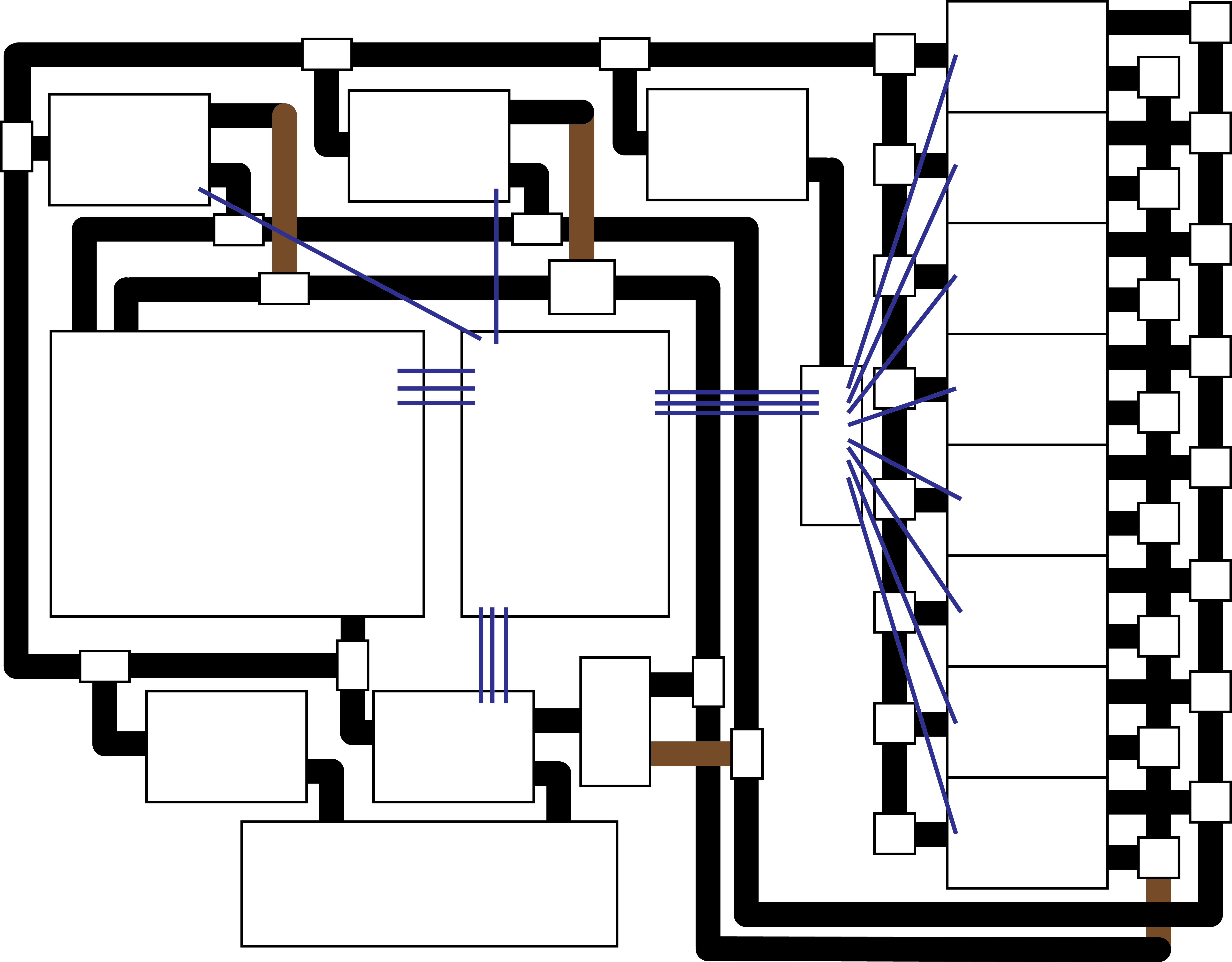
I started to sketch out what the final physical product might look like on a whiteboard, but after the second time of re-drawing the register bank because I wanted it in a different location, I switched to a digital media. I initially got into illustrator and made up a simple block diagram of the components, but then I realized that having that level of abstraction wouldn’t help me sort out errors I would get with real assembly like spacing of cables, joining and splitting of buses, and a bunch of other stuff. So after a bunch of revisions, I ended up with something like this:

|
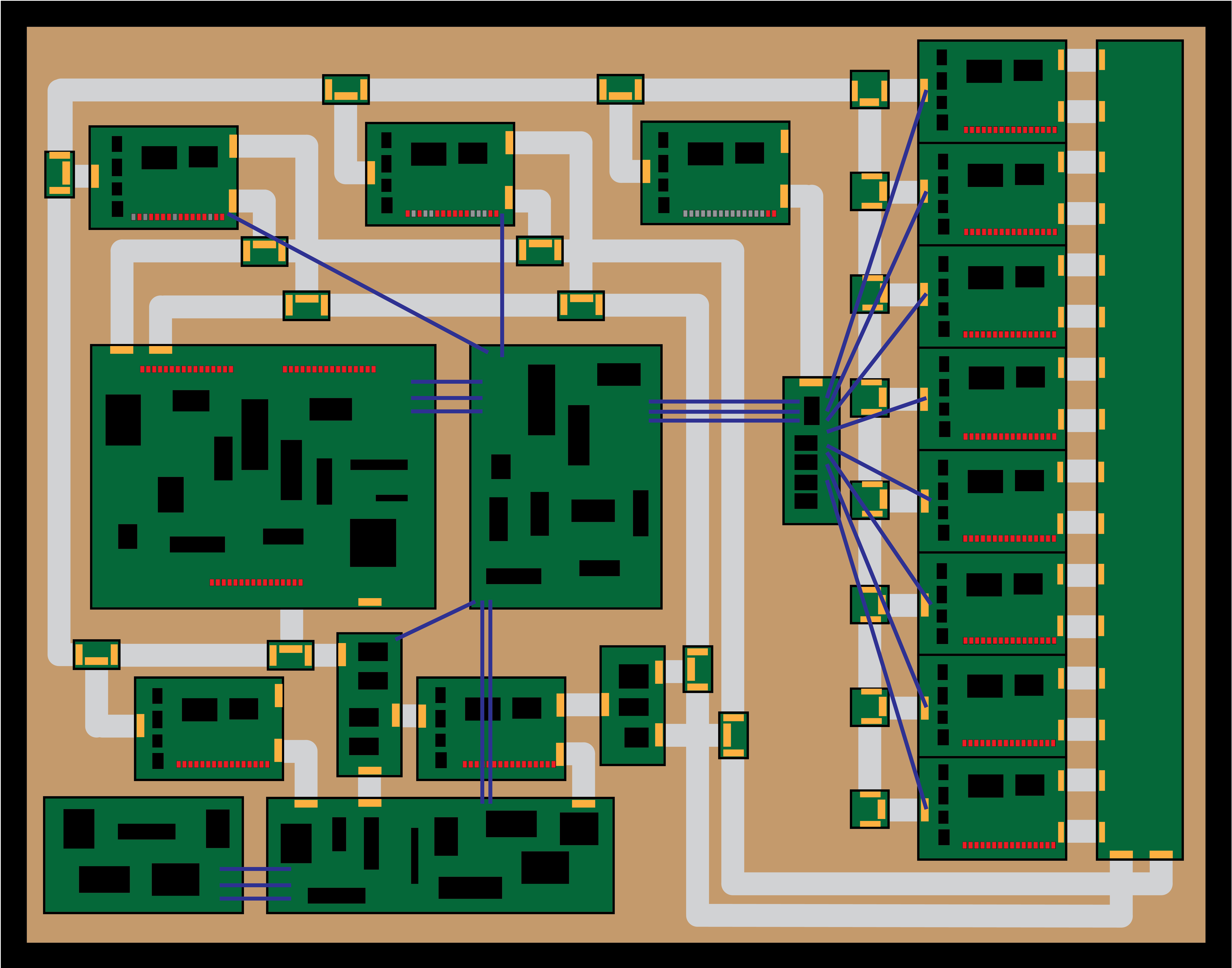
While designing this, I was chatting with my housemate and fellow maker Ethan G., and after asking him a few aesthetics opinion questions he asked me “What is this gonna look like?”. I turned my laptop screen around and showed him the illustrator window containing the figure above, but he pressed further, “No, but I mean what will the final product look like?”. I realized at this point that despite having a great mental image of this final product, I hadn’t put that mental image down concretely anywhere. So, I spent 20 minutes fixing a few things and making my design look more like what the final product would, and ended up with this:

|
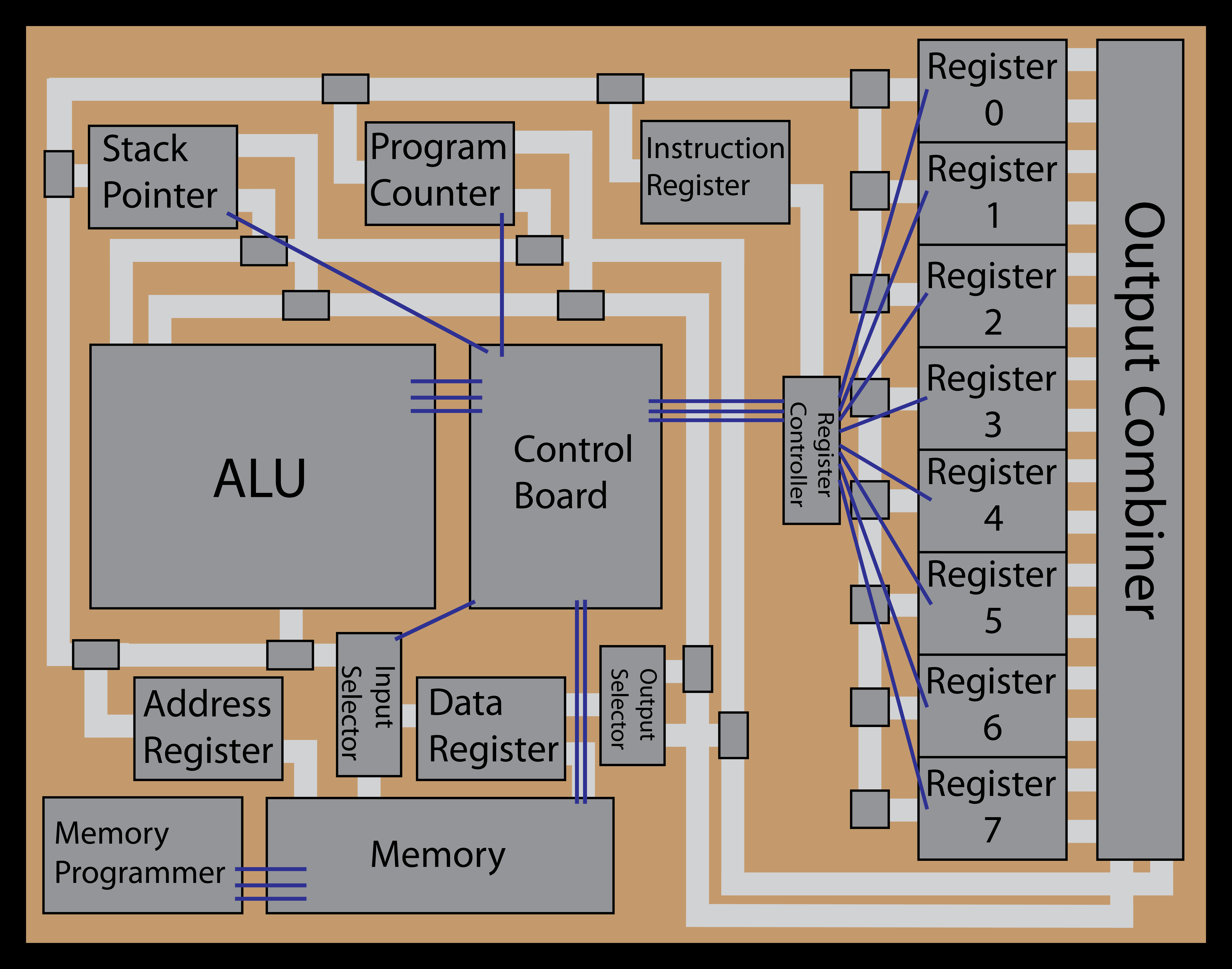
I realized that this can look a bit weird with no context, so enjoy this labeled version as well:

|
First of all, I really like that “final look” image. It makes this whole project feel new and cool again to me after staring at it in Eagle for hours on end. Secondly, it did its job well and made me question a few of the things about my design choices.
The main design choice I questioned was: What if this were just one giant PCB? The main thing that takes up a lot of space in this design is the ribbon cable and the connections between the modules. If I could get rid of all of those connectors, all of those cables, and all of those bus splitters, I could not only cut down on overall size, but also cut down on material cost. There are some downsides though:
- Any failure on a board, from the manufacturer or from me, scraps the whole board or calls for repairs rather than replacement.
- Similarly, I would need to re-order the whole project board if there are any errors in the design, rather than just one board type.
- I would be forced into ordering 5 of the whole project, where as with individual boards, I could have ordered 15 of the register boards to cover the 13 I need, meaning fewer leftovers. Same applies to the bus splitters/joiners.
The good news is that I don’t have to make this decision until the last minute. Even if I combined the design to all be on one board, I would keep the sections separate for educational and visual benefit. That means that should I decide I want to make the project all on one board, I can import the separate boards into eagle, delete the connectors, route the buses, and it will be done. Who knows, if everything works separately and I really like it, I could do it both ways.
The other thing this question forced me to address was “what do I want this to look like?” I fought internally between what I personally find “cool” and the somewhat “retro” look I feel this project deserves. It is also a question I don’t have a concrete answer to at the moment, though I do have a default should no other influencing factors come up. That default would be having mounting holes in each PCB, getting a piece of acrylic or thin wood, mounting all the boards with small standoffs, connecting them with flat flexible cables, and putting the whole thing in some sort of frame. I feel that unless something better comes along or there is some reason not to do it that way, it will feel the appropriate mix of educational, retro, and artsy.
Some other less important things that this exercise thankfully made me realize about the design:
- I should be contentious of where the control signals enter and leave each board for maximum tidiness.
- I didn’t want to deal with the 14 extra cables and 15 extra boards that would come with joining each register to the two output buses individually, so I made one giant board for that purpose. I might do something similar for the input buses, but I can’t decide if it’s worth it. I might just re-use the output bus board.
- I actually need 3 outputs and a separate input bus driver for the memory data register, because apparently everything interacts with it.
- The control-path board should probably have some LEDs on it, though I realized this while writing the blog post, so it won’t be in the picture.
- I haven’t quite tackled it yet, but orientation of signals on the bus is going to be a pain. I think my only hope is to standardize that pin 16 is on the bottom and the right and bend/adapt my cables until they hook up like that.
Anyway, this just confirms what I knew from the start: This is and will continue to be a large project.
-Dillon